Circuit diagram for 4 bit binary adder using ic 7483 » diagram board Ic 7483 pin diagram, truth table, applications 74ls48 bcd-to-7 segment decoder/driver ic in pakistan
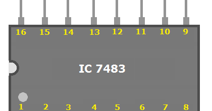
Ic 7483 Pin Diagram Circuit
Design and implementation of a bcd adder circuit using ic-7483
Solved 2. design an adder/subtractor circuit using 7483 and
Ic 7483 pin diagram circuitCircuit diagram for 4 bit binary adder using ic 7483 Circuit diagram for 4 bit binary adder using ic 74837486 ic quad 2-input exclusive-or gate.
Four bit adder or subtractor using 7483Design and implement 9's complement circuit using ic-7483 7486 ic logic xor ttl gate input quad exclusive family partco dip14 datasheet hc electronics fiIc 7483 internal circuit diagram.

Ic 7483 internal circuit diagram
Design and implementation of 10’s complement circuit using ic-7483#4bit_binary_adder_(design, implement and verify the truth table using 7483 4-bit binary full adder icIc 7483 pin diagram circuit.
Bcd subtractor using ic 7483 circuit diagramDesign and implementation of 10’s complement circuit using ic-7483 12+ ic 7420 pin diagramThe counting thread.

7485 comparator ic bit magnitude electronics digital
Ic 7446 datasheet pdfIc 7483 internal circuit diagram Circuit diagram for 4 bit binary adder using ic 748374hc83 full adder ic pinout, datasheet, equivalent working, 50% off.
.


![[DIAGRAM] Logic Diagram Of Ic 7483 - MYDIAGRAM.ONLINE](https://i.ytimg.com/vi/2IoNEBtWGvw/maxresdefault.jpg)